Hardware
India doubles down on chip talent to power semiconductor dream
Semicon 2.0, industry partnerships and new courses aim to power India’s chip
ambitions


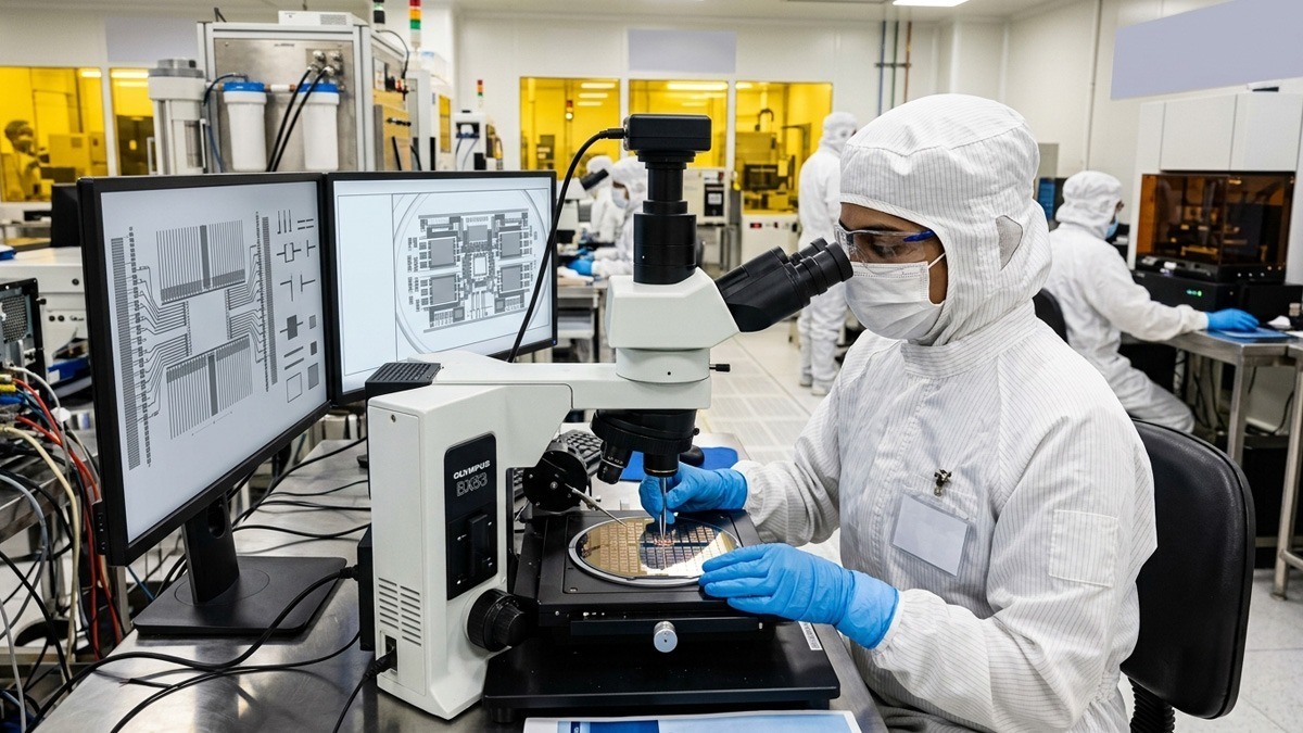
New Delhi: India is laying the building blocks for its semiconductor ambitions by investing as much in people as in plants. As the country pushes to become a global chipmaking hub, the government has rolled out a multi-pronged strategy to develop a skilled workforce across chip design, fabrication and advanced packaging under the Semicon India Programme and the newly approved Semicon 2.0 initiative.
The talent push has already begun to show results. More than one lakh engineers have been trained through government-backed programmes, while nearly 68,000 people have received specialised training in chip design. In addition, 175 chip designs have been successfully taped out from the Semiconductor Laboratory (SCL) in Mohali under the Chips to Startup (C2S) programme.
A major focus has been on integrating semiconductor education into engineering institutions. Through the C2S programme, the government has provided free access to advanced electronic design automation tools, enabling students and researchers to gain hands-on experience with industry-standard chip design software. The tools have collectively recorded more than 240 lakh hours of usage.
To further strengthen the talent pool, the National Institute of Electronics and Information Technology established a Skilled Manpower Advanced Research and Training (SMART) Lab at its Calicut campus. The initiative, aimed at training one lakh engineers in VLSI, embedded systems and the Internet of Things, has already surpassed its target.
Curriculum reforms have also gathered pace. Acting on recommendations from an industry-academia-government committee, the All India Council for Technical Education has introduced new undergraduate, diploma and minor degree programmes focused on semiconductor technologies to ensure graduates are equipped with industry-ready skills.
The government’s efforts extend beyond chip design into semiconductor manufacturing. A new Semiconductor Assembly and Electrostatic Discharge Training Laboratory is being established at NIELIT Guwahati to support the growing Assembly, Testing, Marking and Packaging (ATMP) ecosystem, particularly in the North Eastern region.
Meanwhile, the India Semiconductor Mission has partnered with Lam Research to deliver large-scale training in nanofabrication and process engineering. The collaboration aims to create 60,000 skilled professionals over the next decade to meet the growing demand for advanced manufacturing talent.
Industry partnerships have become another key pillar of the strategy. Through the FutureSkills PRIME platform, jointly run by the Ministry of Electronics and Information Technology and NASSCOM, learners can access online courses covering semiconductors and other emerging technologies.
The India Semiconductor Mission has also signed an agreement with NAMTECH to train around 5,000 professionals over the next five years through certification programmes, internships and apprenticeships across semiconductor fabrication, ATMP facilities and chip design companies.
On the research front, the government has partnered with IBM to establish a semiconductor research centre in India focused on advanced research, intellectual property creation and chip prototyping.
International collaborations are also expanding. Agreements with Purdue University and Arizona State University will support academic exchanges, joint research and workforce development, giving Indian students and researchers greater exposure to global semiconductor expertise.
Backing these initiatives is Semicon 2.0, approved by the Union Cabinet earlier this month with an outlay of Rs 1.275 lakh crore. The programme introduces dedicated funding for research, advanced technologies and talent development across both chip design and manufacturing.
Tamil Nadu has emerged as one of the biggest beneficiaries of the Chips to Startup programme, with more than 60 engineering institutions, including the Indian Institute of Technology Madras, National Institute of Technology Tiruchirappalli, Anna University, Vellore Institute of Technology and SRM Institute of Science and Technology receiving access to advanced chip design tools.
The details were shared by Ministry of Electronics and Information Technology union minister of state Jitin Prasada in a written reply in the Lok Sabha. Together, the initiatives reflect India’s strategy of ensuring that while semiconductor factories may build the chips, it is a skilled workforce that powers the industry’s long-term success.